 by
by
In this tutorial, we introduce a phase lag compensator, and we explain a procedure for designing the parameters of the phase lag compensators. At the end of this tutorial, we give an example of designing the phase lag controller for a second-order system with a low phase margin. Before reading this tutorial, it is a good idea to get yourself familiar with phase lead controllers. You need to read this tutorial and this tutorial.
The effects of the Phase Lag Compensator
- A phase lag compensator increases the phase margin and provides attenuation in the region near and above the gain crossover frequency (high-frequency range). Consequently, the relative stability of the system is improved.
- The gain crossover frequency is decreased and this decreases the bandwidth of the closed-loop system. This usually decreases the rise time and the settling time of the closed-loop system.
- The phase lag compensator approximates a Proportional Integral (PI) controller.
To illustrate the effect of the phase lead controller on the step response, consider the following system.
(1) 
The compensated system is
(2) 
The step responses of the compensated and uncompensated systems are shown in the figure below.
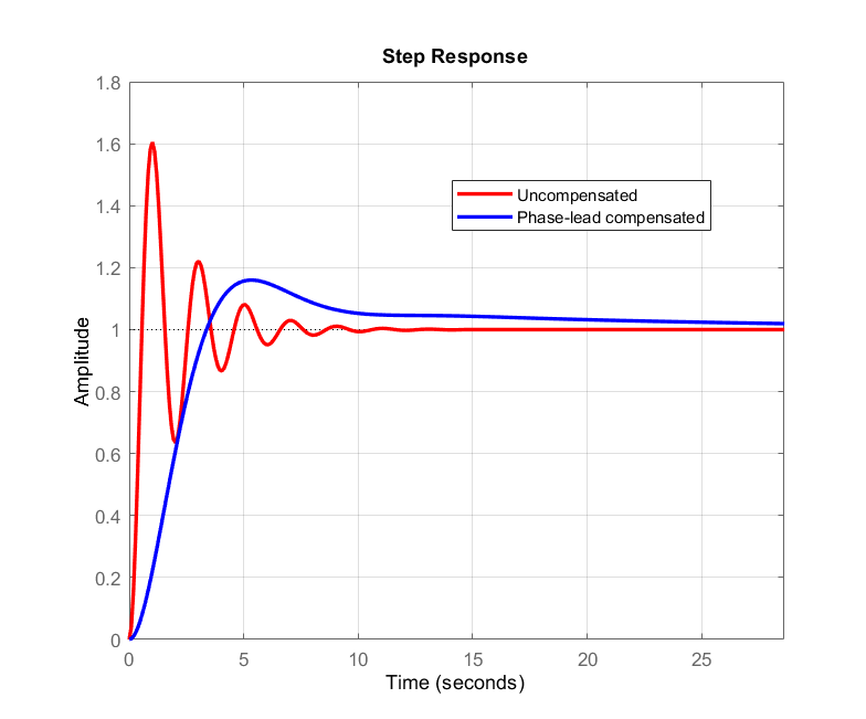
We can observe that the phase lag compensator reduces the damping of the step response and makes the system more stable. However, the price we have to pay is the slower step response.
The figure below graphically illustrates the main idea of the phase lag compensator.
Equations and Graphs Describing the Phase Lag Compensator
The phase lag compensator is described by the following equation:
(3) 
Obviously, it has a similar form to the form of the phase lead compensator, except for the crucial fact that  . We explained the phase lead compensators in our previous tutorial, which can be found here. As mentioned previously, the phase lag compensator approximates a PI controller. It is called a lag compensator because we introduce a phase lag as a side effect in the low frequency range much below the gain crossover frequency. The main purpose of the lag controller is to reduce the gain near gain cross-over frequency, without changing the phase of the original uncompensated system. In this way, we can reduce the gain crossover frequency, and since the phase is not significantly changed, we increase the phase margin (this will become completely clear later). The Bode diagram of the phase lag compensator is shown in the figure below.
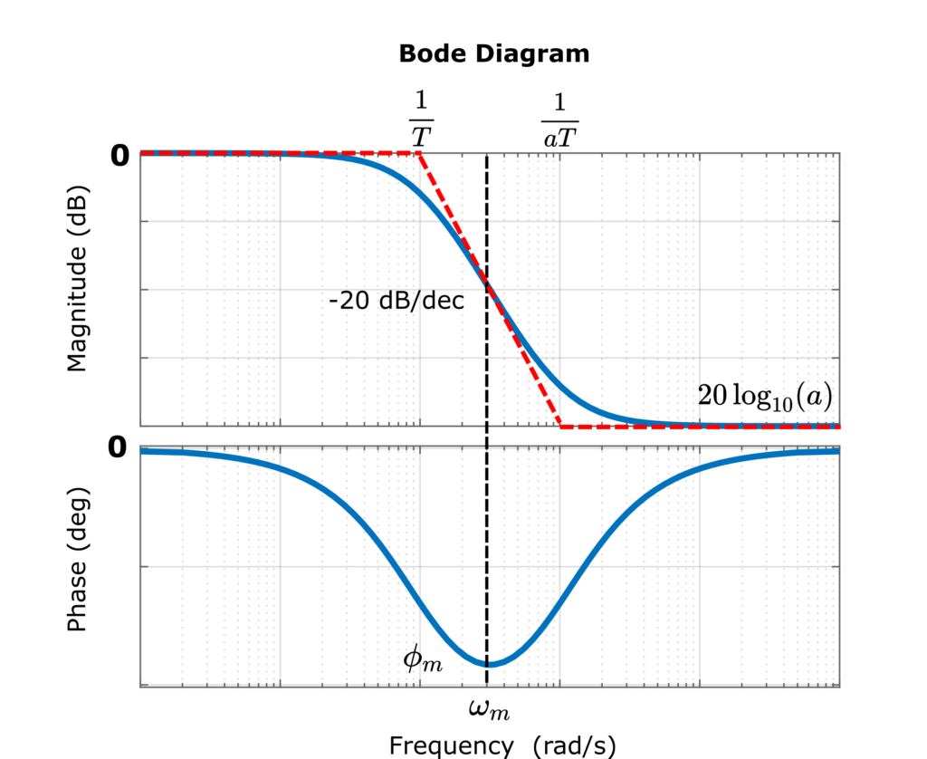
The most important observation from Fig. 3 is the asymptotic negative gain of  . By tuning this gain, we can achieve the main goal of the lag compensator: to increase the phase margin.
Design Procedure for the Phase Lag Compensator
Design specification and goal: Achieve the Phase Margin (PM) of the compensated system that is larger or equal to the minimum desired value of the PM. Design the parameters  and
and  of the lag compensator
(4) 
STEP 1: Plot the Bode diagram of the uncompensated open-loop system. Identify the phase margin of the uncompensated system. Determine the phase margin of the uncompensated system. Under the assumption that the phase margin needs to be increased, identify the frequency on the phase plot, for which the phase margin of the compensated system is 5 to 10 degrees larger than the desired phase margin. Let this frequency be called  . This is the desired gain crossover frequency of the compensated system.
STEP 2: The goal of step 2 is to bring the magnitude curve to  at . In this way, we can achieve the desired design goal. From the Bode magnitude plot, we read the magnitude of the uncompensated system at . Let this magnitude be denoted by
  . On the other hand, from Fig. 3 above we can observe that the lead compensator attenuates the magnitude plot for (under the assumption that is significantly larger than the corner frequency
  of the lag compensator ). Consequently, we want this attenuation to be equal to at . Accordingly, the design equation is
(5) 
where || is the absolute value. From this equation, we obtain the parameter of the phase lag compensator.
(6) 
STEP 3: The next step is to select the parameter . The main idea is to determine the parameter , such that the corner frequency of the lag compensator is significantly smaller than the gain crossover frequency of the compensated system. This has to be done in order to ensure that the phase lag of the compensator will not significantly affect the phase of the compensated system near . However, if we place to be too low, we might decrease the bandwidth of the closed-loop system and consequently, decrease the speed of the response of the closed-loop system. A general rule of thumb is to place one decade below (however, you can also deviate from this rule if your system requires such a compensation). Consequently, we can select the parameter such that it satisfies the following equation
(7) 
Consequently, we have the following equation for the design of the parameter
(8) 
STEP 4: Plot the Bode diagram of the compensated system and see if the desired specifications are met. If not, repeat the step 2,3, 4 by increasing the phase margin, and changing the parameter (you can also deviate from equation (7)).
Example of Designing Phase Lag Controller
PROBLEM: Consider the following open-loop system:
(9) 
Design the lag compensator such that the phase margin of the compensated system is at least 50 degrees.
SOLUTION: We follow the above-described procedure for designing the phase lag controller.
STEP 1: The Bode diagram of the uncompensated system is given below.
The step response of the uncompensated closed-loop system is given in the figure below.
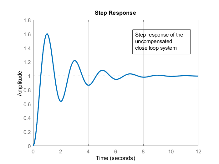
By analyzing the results shown in these two figures, we can conclude that the phase margin does not satisfy the minimum requirement of 50 degrees. Also, from the step response, we can observe that the transient step response is undamped. Our goal is to increase the phase margin by using the phase lag controller. The two figures presented above are generated by using the following MATLAB code lines
clear
W=tf(10,[1 1 0])
figure(1)
bode(W)
grid

figure(2)
WclosedLoopUncompensated=feedback(W,1)
step(WclosedLoopUncompensated)
grid
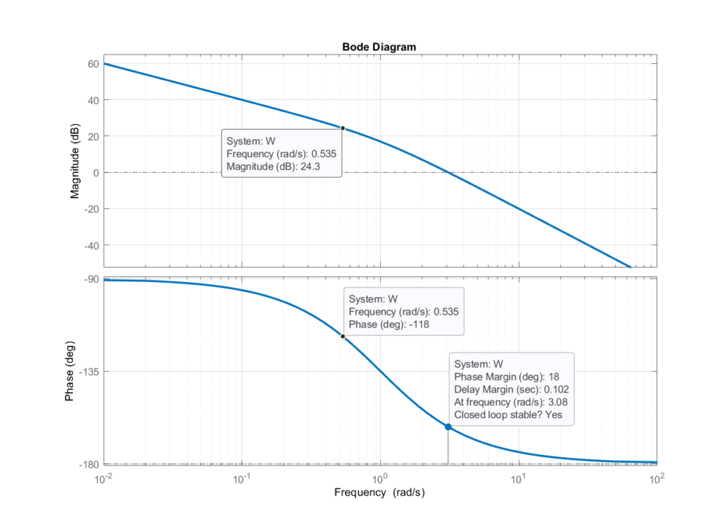
From the Bode plot of the uncompensated system (see the figure above), we choose the gain cross-over frequency of the compensated system as
(10) 
this gain frequency gives the estimated phase margin of the compensated system of 62 degrees, and that is 5 to 12 degrees larger than the desired minimum value of the phase margin.
STEP 2: From the Bode plot of the uncompensated system, we can observe that the necessary attenuation of the -24.3 [dB]. Consequently, we have
(11) 
STEP 3: We select as
(12) 
The final compensator for the computed values of and is
(13) 
The MATLAB code lines used in steps 2 and 3 are shown below.
wc=0.535
Mc=24.3
a=10^(-Mc/20)
T=10/(a*wc)
Gc=tf([a*T 1],[T 1])
STEP 4: The Bode plots of the compensated and uncompensated systems are shown in the figure below.
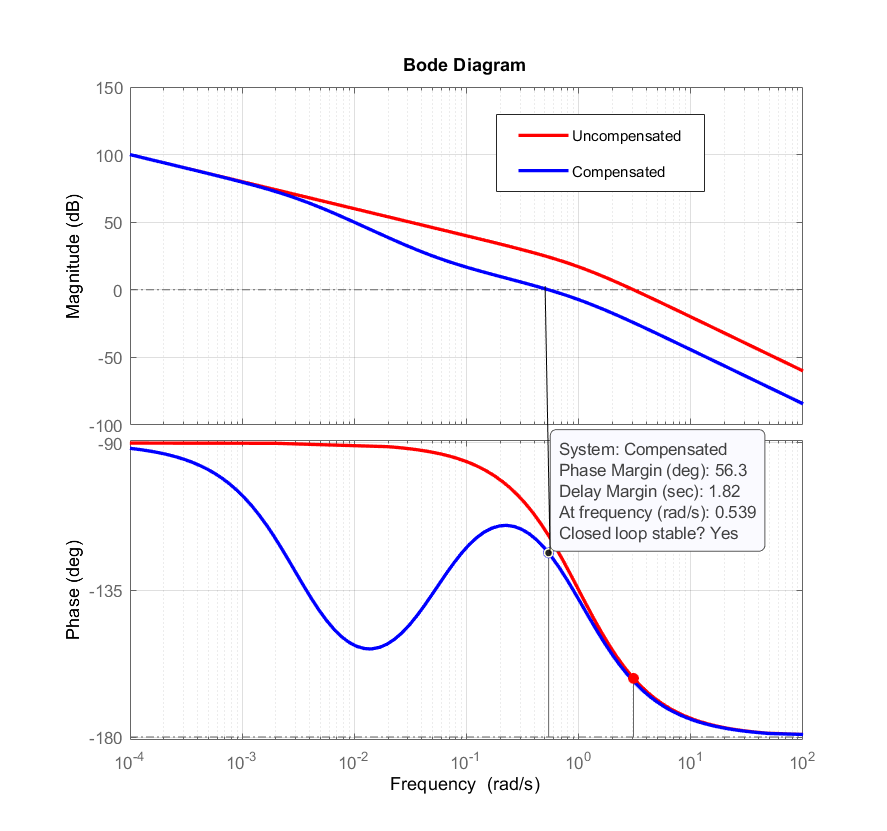
We can observe that the compensated system achieves the required phase margin, and the gain cross-over frequency is close to the estimated one. The figure below shows the step responses of the closed-loop compensated and uncompensated systems.
We can observe that the damping is attenuated, however, at the expense of the slower response. The system will eventually settle in the desired position of  .
.
MATLAB code lines used to generate these two figures are shown below.
figure(3)
hold on
bode(W,'r')
bode(Gc*W,'b')
grid


figure(4)
WclosedLoopCompensated=feedback(Gc*W,1)
hold on
step(WclosedLoopUncompensated,'r')
step(WclosedLoopCompensated,'b')