by
by
In this FPGA and Verilog tutorial, we explain how to generate Pulse Width Modulation (PWM) signals on FPGA using Verilog. The YouTube tutorial is given below.
Basic Circuit and Hardware Connections
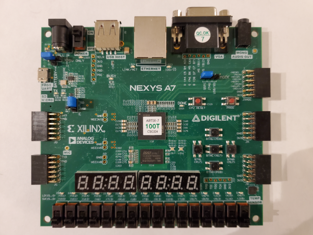
This tutorial is based on Nexys A7 100T (ARTIX-7 100T) FPGA. However, everything explained in this tutorial can be generalized to other FPGAs. The board is shown below.
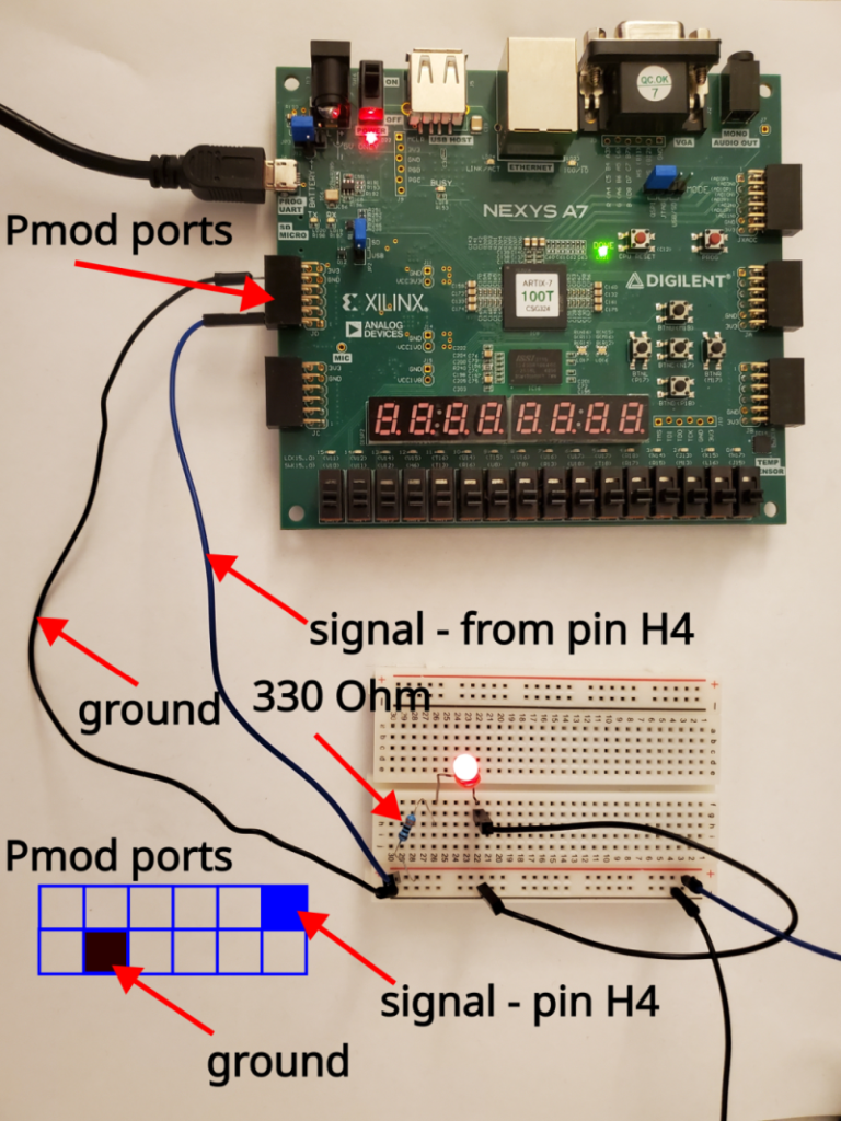
The board connected to a breadboard is given below. We connect the breadboard to the JD Pmod port. The signal wire is connected to pin H4. It is very important to remember the name of this pin. We use a 330 Ohm resistor to limit the current passing through the LED. Pmod ports are shown below. The two wires attached to the right lower corner of the breadboard are oscilloscope wires used to monitor the signal.
Verilog Code of PWM
We are using Vivado and Verilog to implement PWM. Before writing the code, it is very important to obtain the board manual and the board schematics. In our case, the schematics and manual are given here. Namely, in order to write a constraint file, it is necessary to know the pin number of the system clock (used as a reference time) and the pin numbers of the Pmod ports (used to generate output PWM signals).
The Verilog code implementing PWM is given below.
`timescale 1ns / 1ps

module main_file(
    input clk,
    output led
    );

integer counter=0;
// here adjust the period and pulse width
integer periodLength=400000; //  periodLength times 10 10^(-9)(this is the clock in seconds) = period length in seconds
integer  pulseLength=200000; // use the same formula to get seconds
always@(posedge clk) begin

    if (counter<periodLength) counter<=counter+1;

    else counter<=0;

end

assign led=(counter<pulseLength) ? 1:0;

endmodule
This module has two inputs:
- “clk” – this is the clock input. This input will be connected (constrained to) the clock of the system. The board Nexys A7 has a clock of 100 MHz. This info can be found in the documentation of the board (section 5 called “Oscillators/Clocks” ). This means that the clock period is 10 nanoseconds.
- “led” – is the signal output. This output will be connected to the pin H4 of the JD Pmod port (see the second figure). This output is our PWM signal.
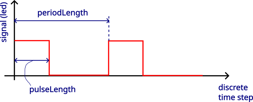
In this code, we are generating PWM signals with a period of 4 miliseconds and with a pulse width of 2 milliseconds (here, we select different parameters compared to the YouTube tutorial). The period of the signal expressed in discrete-time steps is denoted by “periodLength” in the code. Every time step (basic unit) is determined by the period of the system clock. In our case, the period of the system clock is 10 nano seconds. The pulse width (length) expressed in discrete-time steps is denoted by “pulseLength”. The PWM signal in discrete time steps is illustrated in the figure below
We can convert the duration of the “periodLength” and “pulseLength” from discrete-time steps to total time as follows:
(1) 
where  is the period of the system clock. Similarly, we can express “pulseLength” in seconds. Obviously, you can change the parameters “periodLength” and “pulseLength” to achieve any desired shape of the PWM signal.
Let us now go back to our code. The variable “counter” goes from zero to “periodLength” in the “always” block. The triggering event for the “always” block is a positive edge of the “clk” variable. That is, when the “clk” variable changes its value from low to high, the “always” block will be triggered. The system clock is shown in the figure below (top train of pulses). This figure is generated by using a Verilog simulation (more about this in our future tutorials).
In the always block, the “counter” variable is either incremented or set back to zero if the counter reaches the end of the period. This process is repeated continuously since all the statements and assignments in the “always” block are non-blocking.
The statement
“assign led=(counter<pulseLength) ? 1:0;”
will assign the output “led” to 1 if the counter is smaller than “pulseLength”, otherwise, the value of “led” is set to zero.
The next step is to define the constraint file. The constraint file is given below.
set_property PACKAGE_PIN E3 [get_ports {clk}]
create_clock -name sysclk -period 10 [get_ports {clk}]
set_property IOSTANDARD LVCMOS33 [get_ports {clk}]

set_property PACKAGE_PIN  H4 [get_ports {led}]
set_property IOSTANDARD LVCMOS33 [get_ports {led}]
From section 5 of the board manual , we concluded that the system clock is connected to the pin E3. Consequently, E3 is used to constrain the “clk” input. The second code line is used to specify the code period of 10 ns. From section 10 of the board manual, we concluded that the signal wire is connected to the pin H4 of the JD Pmod port. Other code lines are standard. If you have a different board, you need to find online the board manual and board documentation, and you need to find the correct pin numbers for the clock and the signal port.
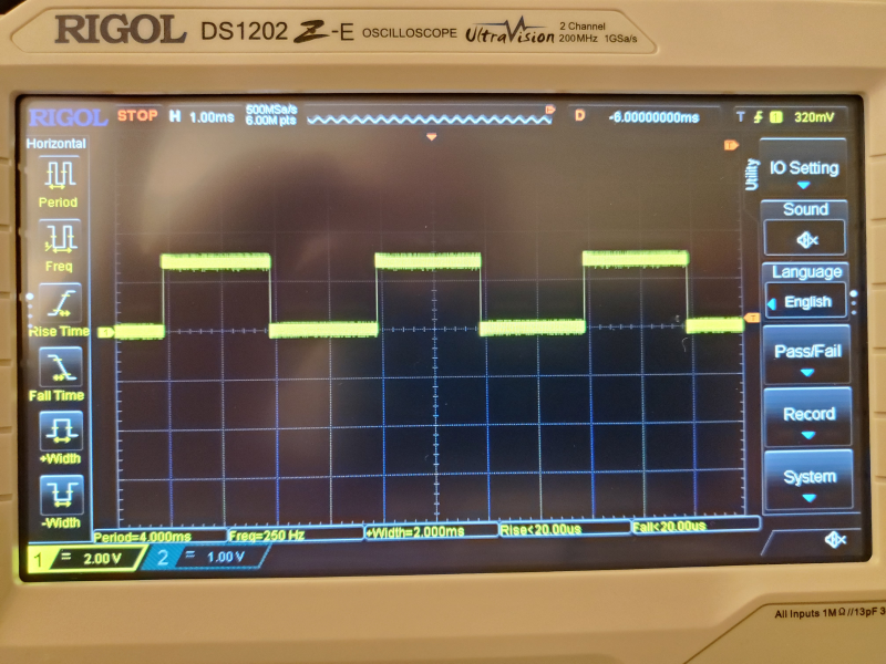
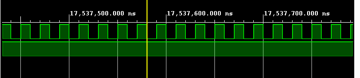
After saving the module and constraint files you need to generate a bitstream and program the board. The generated signal measured by an oscilloscope is shown in the figure below. We can see that we can accurately control the PWM signal period and width.