– In this FPGA tutorial, we explain how to define and use hardware clocks in Verilog and Vivado. As a demonstration, we explain how to generate a Pulse Width Modulation (PWM) signal with precisely controlled frequency and duty cycle.
– In this tutorial, we are using Nexys A7 100T FPGA. This is a very popular FPGA that is often used in electrical and computer engineering programs in the US and Europe. However, everything explained in this tutorial can easily be used in the case of other FPGAs.
The YouTube tutorial is given below.
How to Define Define and Use Hardware Clocks in FPGA, Vivado, and Verilog
– The first step is to find the FPGA board specifications and investigate what types of clocks the FPGA board provides as well as the clock pin names and numbers. The Nexys A7 100T board includes a single 100 MHz crystal oscillator clock connected to pin E3 (The clock specifications can be found here, in Section 6). This means that the period of the clock is 10 nanoseconds, and we need to specify the hardware pin E3 in the xdc constraint file.
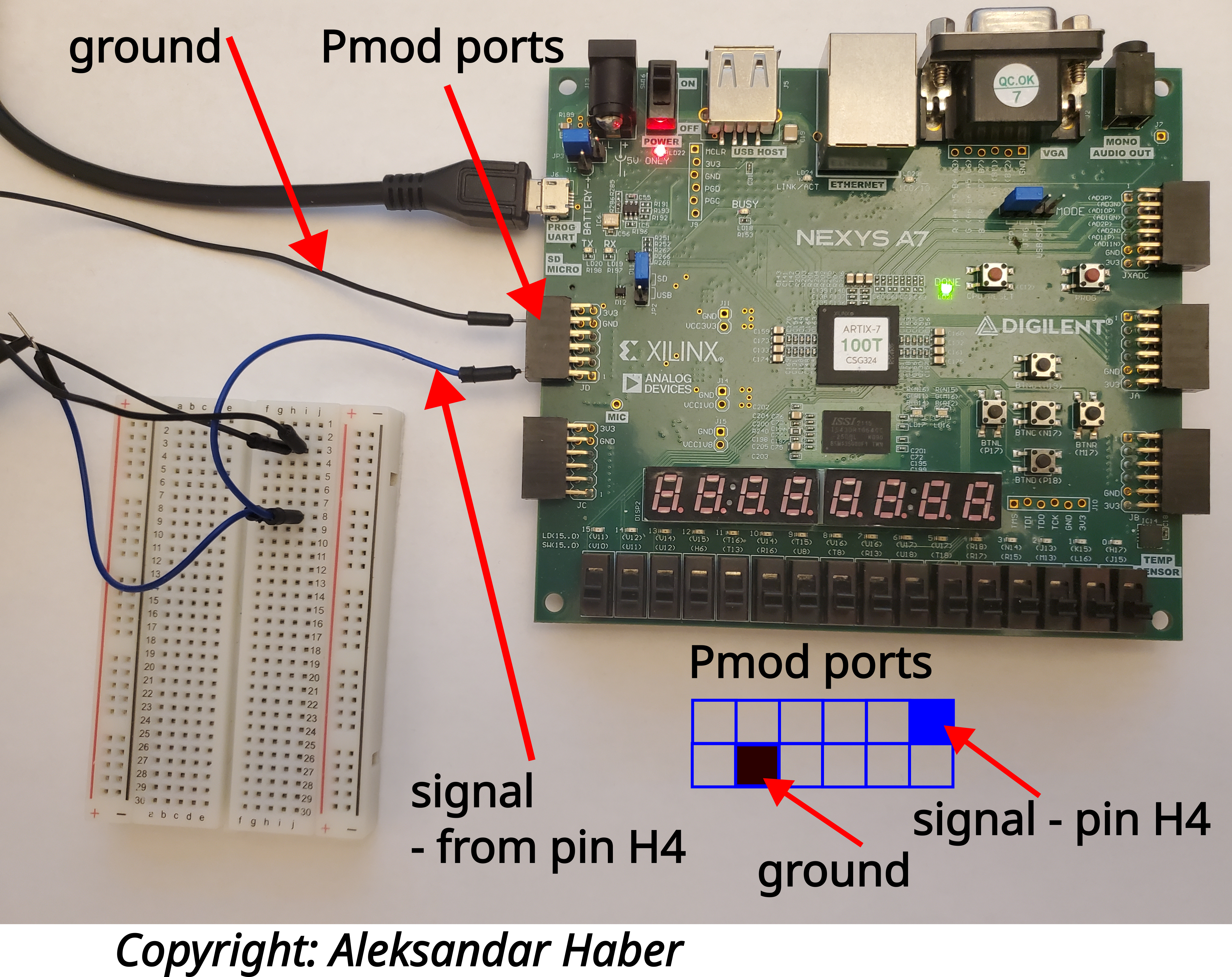
As a test, we will use the clock to generate a Pulse Width Modulation (PWM) signal of a desired period (frequency) and a pulse width. The wiring diagram is shown below.

We use the Pmod port near the USB/UART connector. We use the pin H4 of this Pmod port to generate the PWM signal. Then, we use the ground pin on the same port to close the circuit. The pin locations are shown in the figure above. We have attached oscilloscope probes to the pin H4 and the ground pin by using a breadboard.
We first create a Vivado project, and then, we create a constraint file shown below.
set_property PACKAGE_PIN E3 [get_ports {CLK}];
create_clock -name sysclk -period 10 -waveform {0 5} [get_ports {CLK}];
set_property IOSTANDARD LVCMOS33 [get_ports {CLK}];

set_property PACKAGE_PIN  H4 [get_ports {SIGNAL}];
set_property IOSTANDARD LVCMOS33 [get_ports {SIGNAL}];
In the sequel, we explain this file line by line. The first code line:
set_property PACKAGE_PIN E3 [get_ports {CLK}];connects a port called “CLK” with the hardware clock pin E3. Later on, we will declare and define the input port called “CLK” in the main module. Next, we create a hardware clock by using this statement:
create_clock -name sysclk -period 10 -waveform {0 5} [get_ports {CLK}];The name of the clock is “sysclk” and the period is 10 nanoseconds. Then, we define a waveform by using this notation {0 5}. The number 0 means that the rise edge should happen at 0 nanoseconds, and the number 5 means that the fall edge should happen at 5 nanoseconds. Finally, we connect the defined clock with the port named CLK (that will be declared later on in the main module). The next line is a standard line that specifies IOSTANDARD for CLK port:
set_property IOSTANDARD LVCMOS33 [get_ports {CLK}]; The next line:
set_property PACKAGE_PIN H4 [get_ports {SIGNAL}];connect the port called SIGNAL (that will be declared later on in the main module) with the pin H4. This is the Pmod pin in the wiring figure above. The next line is a standard line that defines IOSTANDARD:
set_property IOSTANDARD LVCMOS33 [get_ports {SIGNAL}]; Next, we write a Python code that calculates the period of the PWM signal and the pulse width.
'''
define a pulse width modulation signal with the period of
5000 nanoseconds ( (1/(5000*10**(-9)))= frequency of 200,000 Hz)
and a duty cycle of 50 % percent

'''
import numpy as np

# FPGA clock period in nanoseconds
periodFPGA=10

# desired period of the PWM signal in nanoseconds
periodPWM= 5000

# duty cycle of the PWM signal, 0-1
dutyCyclePWM=0.5

# pulse width in nanoseconds
widthPWM=int(dutyCyclePWM*periodPWM)

# get the values in clock cycles, every clock cycle is periodFPGA

periodLength=int(periodPWM/periodFPGA)

pulseLength=int(widthPWM/periodFPGA)
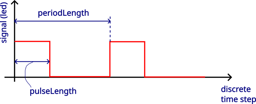
This code calculates the period of the PWM signal, denoted by “periodLength”, and the pulse length (pulse width), denoted by “pulseLength” and expresses these two quantities in the units of clock cycles (clock-pulse units). These two quantities are illustrated in the figure below.

Every discrete-time step in the above figure represents a single period of the hardware clock that is denoted by CLK port in our design. The code calculates (for a desired duty cycle of 50 percent):
periodLength=500
pulseLength=250
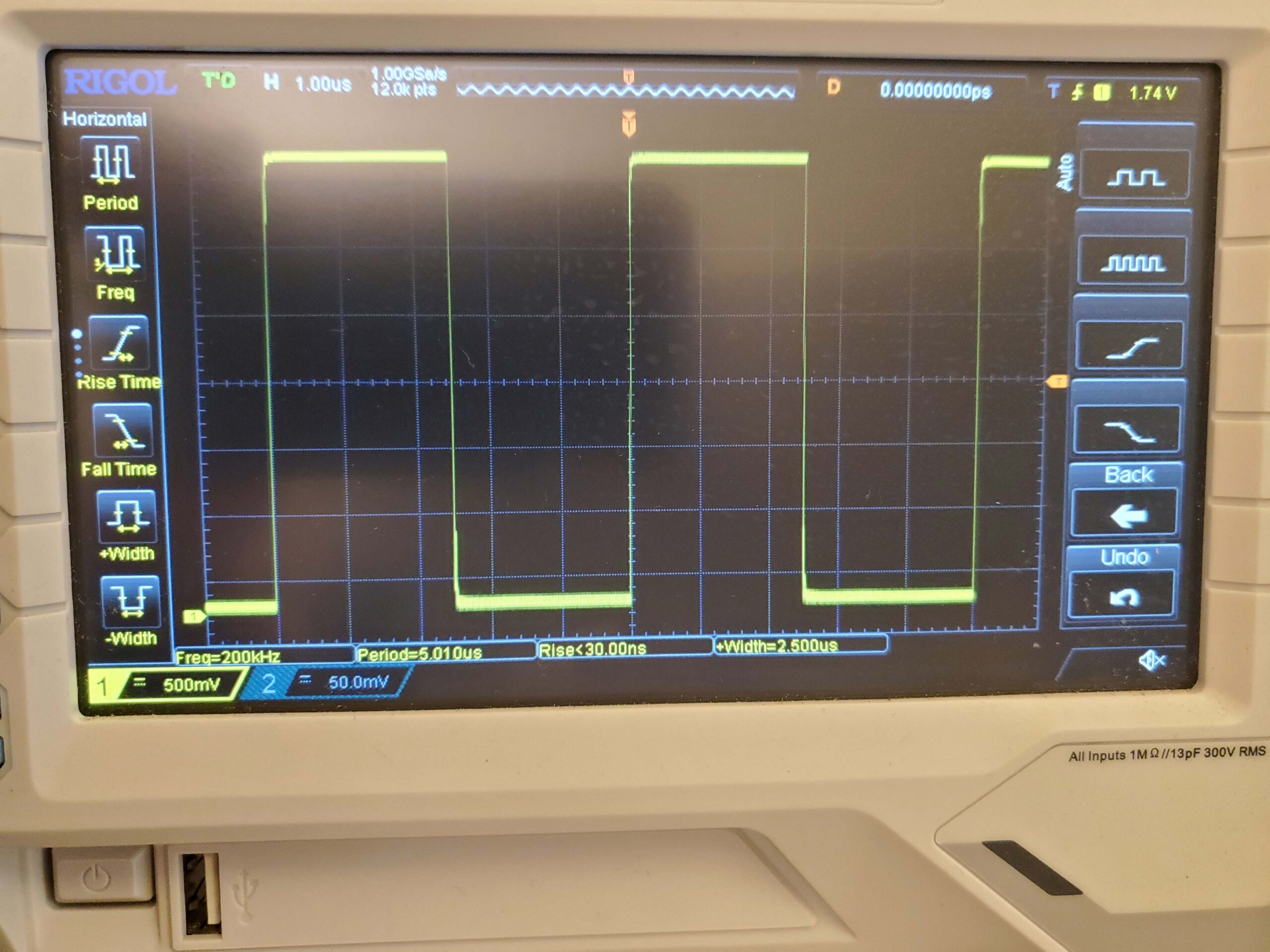
This means that the PWM period is 500 clock cycles long and the pulse width is 250 clock cycles long. Since the duration of a single clock cycle (clock period) is 10 nanoseconds, this means that the PWM period is 5,000 nanoseconds and pulse width is 2500 nanoseconds. This produces a PWM frequency of 200,000 Hz.
The Verilog module that generates the PWM signal on the basis of the defined PWM signal is shown below.
`timescale 1ns / 1ps
module main_module(input CLK, output SIGNAL);
    // period of the PWM signal expressed in clock cycles
    // multiply this value by the clock period to get
    // the value in nanoseconds
    integer periodLength=500;

    // pulse width of the PWM signal expressed in clock cycles
    // multiply this value by the clock period to get
    // the value in nanoseconds
    integer pulseLength=250;

    // this counter is used to create the PWM signal
    integer counter=0;

    // this is used to reset the counter
    always @(posedge CLK)
    begin
        if (counter<periodLength) counter<=counter+1;
        else counter<=0;
    end

assign SIGNAL =(pulseLength>counter) ? 1'b1:1'b0;

endmodule
The code block under the always statement is executed on every rising edge (positive edge, denoted by “posedge”) of the CLK variable (clock input port). In this way, we time our code and control its execution on the basis of the defined clock cycles.
We use the always statement to reset the counter called “counter” when the clock pulses denoted by CLK reach the total number of clock pulses (clock cycles) in a single PWM period. In this way, we have defined an integer that iterates through the discrete-time samples of a single pulse. When the next pulse comes, the integer is set to 0 and the counting starts again. Then, we simply assign SIGNAL value to be high when the counter is smaller than the pulse width, otherwise, the SIGNAL value is low. This produces a train of pulses shown in the oscilloscope reading below.
