In this FPGA tutorial, we explain how to control DC motors by using FPGA, Verilog, and Vivado. We explain how to control DC motors by generating Pulse Width Modulation (PWM) signals that control the rotation speed and by generating two digital signals that control the direction of rotation.
In this tutorial, we are using Nexys A7 100T FPGA. This is a very popular FPGA that is often used in electrical and computer engineering programs in the US and Europe. However, everything explained in this tutorial can easily be used in the case of other FPGAs.
The YouTube tutorial is given below.
Copyright Notice and Code License
Copyright notice: this tutorial, webage, video lesson, developed code files, and documents should not be copied, redistributed, or posted on public or private websites, public or private code repositories, or social media platforms. This lesson and all the provided study materials are strictly for personal use. Without the permission of the author, this lesson and the provided material should not be used for commercial purposes and for training of engineers working in companies. This lesson and the provided material should not be used as lecture materials on online learning platforms and in university courses. This lesson and the provided material should not be used to train an AI algorithm or a large language model. Without the permission of the author, the provided code should not be used for academic research or for commercial purposes.
How to Control DC motors Using FPGA, Vivado, and Verilog
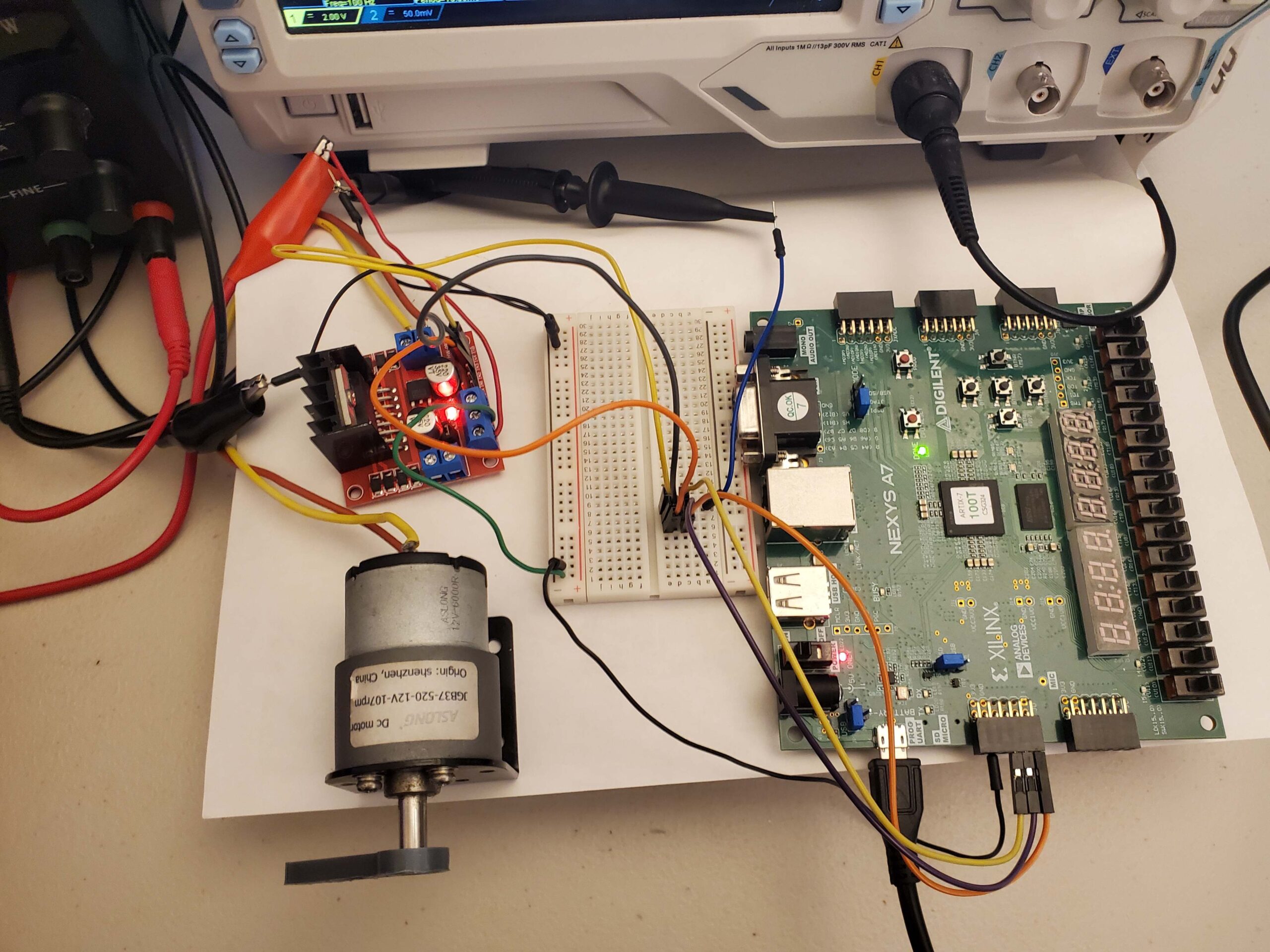
The experimental setup is given below.

We are using
- Nexys A7 100T FPGA. To send the control signals, we are using the JD pmod ports located close to the UART/USB port. Below, we give a wiring diagram.
- JGB37‑520 12V low-cost DC motor. You can also use any other DC motor that is controlled by using PWM signals.
- L298N motor driver. This is a low-cost motor driver that is often used in robotics and mechatronics projects.
- Breadboard, oscilloscope and a power supply providing 12 V of DC power.
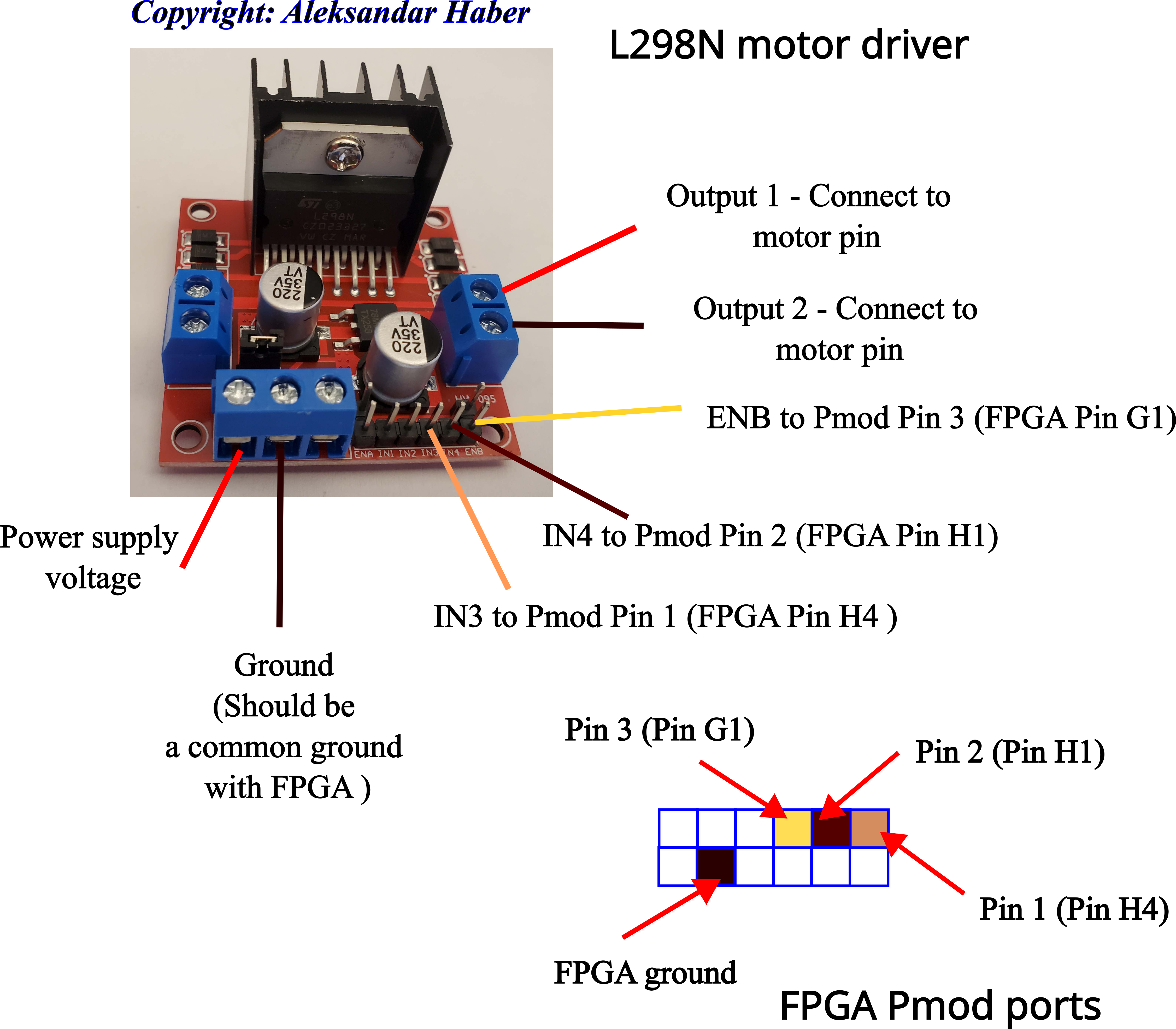
The wiring diagram of the motor driver and FPGA is given below.

The L298N driver has three ports:
- Power supply port. The power supply should be connected to the two pins of the port. The ground pin should be connected to the ground of the FPGA.
- Control port. The control port contains three pins: IN3, IN4, and ENB. The IN3 pin should be connected to the Pin 1 of the Pmod port (H4 hardware pin of FPGA from the board schematics). The IN4 pin should be connected to the Pin 2 of the Pmod pin (H1 hardware pin of FPGA from the board schematics). The ENB pin should be connected to the Pin 3 of the Pmod port (G1 hardware pin of FPGA from the board schematics). The pins IN3 and IN4 are used to control the direction of rotation of the motor. The pin ENB is the PWM pin that is used to control the speed of rotation.
- DC motor port. This port contains two pins. The two pins should be connected to the DC motor.
The JD Pmod port contains 12 pins. We are using pin 1 (H4 hardware pin), pin 2 (H1 hardware pin), pin 3 (G1 hardware pin), and ground pin (see the figure above). Pin 1 is connected to the IN3 pin of the motor driver. Pin 2 is connected to IN4 pin. Pin 3 is connected to the ENB pin of the motor driver.
The pins IN3 and IN4 are used to turn ON or OFF the motor and to control the direction of the motor rotation in this way:
•Motor OFF: IN3-LOW and IN4-LOW (apply a low voltage to IN3 and IN4)
•Motor OFF: IN3-HIGH and IN4-HIGH (apply a high voltage to IN3 and IN4)
•Motor ON and clockwise rotation: IN3-HIGH and IN4-LOW (apply a high voltage to IN3 and low voltage to IN4)
•Motor ON and counterclockwise rotation: IN3-LOW and IN4-HIGH (apply a high voltage to IN3 and low voltage to IN4)
To control the motor, the user is supposed to use the three FPGA push switches: switch 1, switch 2, and switch 3 (connected to the FPGA hardware pins J15, L16, and M13, respectively).
- Switch 1 is used to turn on the motor.
- Switch 2 is used to change the direction of rotation of the motor. If switch 2 is OFF, then the motor turns clockwise. If switch 3 is ON, then the motor turns counterclockwise.
- Switch 3 is used to change the speed of the motor. Is switch 3 is OFF, then the speed is low. If switch 3 is ON, then the speed is high.
For more details, you can see the YouTube video given above.
The first step when implementing the control algorithm in Verilog and Vivado is to write the constraint file. The constraint file is given below.
## clock
set_property PACKAGE_PIN E3 [get_ports {CLK}];
create_clock -name sysclk -period 10 -waveform {0 5} [get_ports {CLK}];
set_property IOSTANDARD LVCMOS33 [get_ports {CLK}];

## motor pins - Pmod
## IN3
set_property -dict {PACKAGE_PIN H4 IOSTANDARD LVCMOS33} [get_ports {MOTOR[0]}];
## IN4
set_property -dict {PACKAGE_PIN H1 IOSTANDARD LVCMOS33} [get_ports {MOTOR[1]}];
## ENB
set_property -dict {PACKAGE_PIN G1 IOSTANDARD LVCMOS33} [get_ports {MOTOR[2]}];

## switches for controlling the motor
set_property -dict {PACKAGE_PIN J15 IOSTANDARD LVCMOS33} [get_ports {SWITCH[0]}];
set_property -dict {PACKAGE_PIN L16 IOSTANDARD LVCMOS33} [get_ports {SWITCH[1]}];
set_property -dict {PACKAGE_PIN M13 IOSTANDARD LVCMOS33} [get_ports {SWITCH[2]}];
The first several lines of the constraint file define the clock and clock pins. The information about the period of the clock as well as the hardware pin for the clock (pin E3) are taken from the board schematics. The name of the port for the clock that will be used in a Verilog module is “CLK” (the Verilog module that implements the control algorithm is stated later on). The physical FPGA clock has a period of 10 nanoseconds, or equivalently, the frequency of 100 Hz.
Then, the next 3 code lines (not counting comments) connect the hardware pins and ports for controlling the motor. Namely, to control the motor, we need to send 3 binary digital signals to the pins H4 (controlling IN3 of the motor driver), H1 (controlling IN4 of the motor driver), and G1 (controlling ENB of the motor driver). To achieve this, the Verilog module we declare a 3-bit wide output port whose name is MOTOR. Consequently, the 3 code lines of the constraint file are used to constraint the output port MOTOR to the hardware pins H4, H1, and G1.
The last 3 lines of the constraint file, define the connections between the hardware pins and the input port called SWITCH. This input port is 3 bit wide and is used to read the information from the physical FPGA switches.
The Verilog module that defines the control algorithm is given below.
`timescale 1ns / 1ps
module main_module(input CLK, input [2:0] SWITCH, output [2:0] MOTOR);

    reg [2:0] control =3'b000;
    // control[0] - IN3
    // control[1] - IN4
    // control[2] - speed : speed LOW - 0 and speed HIGH - 1

    // period of the PWM signal expressed in clock cycles
    // multiply this value by the clock period to get
    // the value in nanoseconds
    integer periodLength=1000000;

    // pulse width of the PWM signal expressed in clock cycles
    // multiply this value by the clock period to get
    // the value in nanoseconds
    integer pulseLength1=200000;
    integer pulseLength2=900000;
    integer pulseLength=0;

    // this counter is used to create the PWM signal
    integer counter=0;

    // this is used to reset the counter
    always @(posedge CLK)
    begin
        if (counter<periodLength) counter<=counter+1;
        else counter<=0;
    end

    always @(SWITCH)
    begin
    casez(SWITCH)
    // no control
    3'b??0: begin
                control=3'b000;
            end
    // control, clockwise, low speed
    3'b001: control=3'b001;

     // control, clockwise, high speed
    3'b101: control=3'b101;

    // control, counterclockwise, low speed
    3'b011: control=3'b010;

    // control, counterclockwise, high speed
    3'b111: control=3'b110;

    default: control=3'b000;

    endcase
    //adjust the speed
    if (control[2]==1'b0)
        pulseLength=pulseLength1;
    else
        pulseLength=pulseLength2;
    end


assign MOTOR[0] = control[0];
assign MOTOR[1] = control[1];
assign MOTOR[2] =(pulseLength>counter) ? 1'b1:1'b0;

endmodule
The input port “CLK” is connected to the hardware clock that has the frequency of 100 Hz. The 3-bit wide input port called “SWITCH” is used to read the user input. For example, if the user presses the first, and second switch, while the third switch is OFF, then, switch becomes SWITHC=110. The 3-bit wide output port called MOTOR is used to control the motor. The first bit of MOTOR corresponds to IN3, the second bit corresponds to IN4, and the last bit corresponds to ENB.
The reg variable called “control” is 3 bit wide and its bits are assigned on the basis of the user input that is encoded in the port SWITCH. The casez statement is used to fill in the bits of control on the basis of SWITCH bits.
To define the PWM signals we declare several integers. The integer called “periodLength” defines the period of the PWM signal expressed in the clock cycle period. That is, the value of “periodLength” should be multiplied by 10 do obtain the period of the PWM signal in nanoseconds. The value of “periodLength” in the code defines a PWM signal with the period of 10 miliseconds which is a PWM signal with the frequency of 100 Hz. Then, the integers “pulseLength1” and “pulseLength2” define the pulse lengths (pulse width) of PWM signals expressed in the clock cycle period. They define two rotation velocities that are selected by selecting the third bit of SWITCH port (SWITCH[2] bit). “pulseLength1” (SWITCH[2]=0) corresponds to low speed and “pulseLength2” corresponds to high speed (SWITCH[2]=1). The integer “pulseLength” is the final value of the pulse length variable that can either be equal to “pulseLength1” or “pulseLength2”. The value of “pulseLength1” defines a duty cycle of 20 percent and the value of “pulseLength2” defines a duty cycle of 90 percent.
Next, we declare a counter variable called “counter”. This variable is used to define a counter that iterates through a single period of the PWM signal. It starts at 0 and it counts until periodLength-1, and then it is being set to 0 and the counting starts again. This is achieved by the first always statement that is triggered on every positive edge of the clock.
The second always statement that is triggered by changing the bits of SWITH and the casez statement are used to fill-in the value of control register on the basis of the SWITCH bits. The bit “control[2]” is used to set the low or high motor speed. The if statement is used to select the correct value of the pulse width.
Finally, we use the last three assign statements to assign the bits of the MOTOR control variable. The least assign statement sets the PWM value HIGH or LOW on the basis of the relation between counter and “pulseLength”. If “counter” is smaller than “pulseLength”, then MOTOR[2] is HIGH, otherwise is LOW.
Below is the Python code that can be used to quickly compute “periodLength” and “pulseLength”
'''
define a pulse width modulation signal with the period of
5000 nanoseconds ( (1/(5000*10**(-9)))= frequency of 200,000 Hz)
and a duty cycle of 50 % percent

'''
import numpy as np

# FPGA clock period in nanoseconds
periodFPGA=10

# desired period of the PWM signal in nanoseconds
periodPWM= 100000

# duty cycle of the PWM signal, 0-1
dutyCyclePWM=0.5

# pulse width in nanoseconds
widthPWM=int(dutyCyclePWM*periodPWM)

# get the values in clock cycles, every clock cycle is periodFPGA

periodLength=int(periodPWM/periodFPGA)

pulseLength=int(widthPWM/periodFPGA)